Products
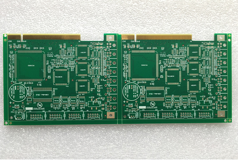
4 layer pcb with gold finger in digital audio system
| Layers | 4 layers |
| Board thickness | 1.60MM |
| Material | FR4 tg150 |
| Copper thickness | 1 OZ(35um) |
| Surface Finish | ENIG Au Thickness 1um; Ni Thickness 3um |
| Min Hole(mm) | 0.203mm |
| Min Line Width(mm) | 0.15mm |
| Min Line Space(mm) | 0.15mm |
| Solder Mask | Green |
| Legend Color | White |
| Mechanical processing | V-scoring, CNC Milling(routing) |
| Packing | Anti-static bag |
| E-test | Flying probe or Fixture |
| Acceptance standard | IPC-A-600H Class 2 |
| Application | Automotive electronics |
Product Material
As a supplier of various PCB technologies, volumes, lead time options, we have a selection of standard materials with which a large bandwidth of the variety of types of PCB can be covered and which are always available in house.
Requirements for other or for special materials can also be met in most cases, but, depending upon the exact requirements, up to about 10 working days may be needed to procure the material.
Do get in touch with us and discuss your needs with one of our sales or CAM team.
Standard materials held in stock:
|
Components |
Thickness | Tolerance |
Weave type |
|
Internal layers |
0,05mm | +/-10% |
106 |
|
Internal layers |
0.10mm | +/-10% |
2116 |
|
Internal layers |
0,13mm | +/-10% |
1504 |
|
Internal layers |
0,15mm | +/-10% |
1501 |
|
Internal layers |
0.20mm | +/-10% |
7628 |
|
Internal layers |
0,25mm | +/-10% |
2 x 1504 |
|
Internal layers |
0.30mm | +/-10% |
2 x 1501 |
|
Internal layers |
0.36mm | +/-10% |
2 x 7628 |
|
Internal layers |
0,41mm | +/-10% |
2 x 7628 |
|
Internal layers |
0,51mm | +/-10% |
3 x 7628/2116 |
|
Internal layers |
0,61mm | +/-10% |
3 x 7628 |
|
Internal layers |
0.71mm | +/-10% |
4 x 7628 |
|
Internal layers |
0,80mm | +/-10% |
4 x 7628/1080 |
|
Internal layers |
1,0mm | +/-10% |
5 x7628/2116 |
|
Internal layers |
1,2mm | +/-10% |
6 x7628/2116 |
|
Internal layers |
1,55mm | +/-10% |
8 x7628 |
|
Prepregs |
0.058mm* | Depends on layout |
106 |
|
Prepregs |
0.084mm* | Depends on layout |
1080 |
|
Prepregs |
0.112mm* | Depends on layout |
2116 |
|
Prepregs |
0.205mm* | Depends on layout |
7628 |
Cu thickness for internal layers: Standard – 18µm and 35 µm,
on request 70 µm, 105µm and 140µm
Material type: FR4
Tg: approx. 150°C, 170°C, 180°C
εr at 1 MHz: ≤5,4 (typical: 4,7) More available on request
Stackup
The 4 layer printed circuitboard stackup is having 3 of the single layers and a ground layer making it4 layers in total.
All these layers are used for the routing of signals.
The frst two inner lavers are lying inside the core and are often utillized as the power panes or are commonly referred to as routing of signals.
Simply speaking a 4-layer PCB stackup is having 2 of the singlea VCC and a ground layer.

Key points for pcb purchasing
Most electronics factory purchasers have been confused about the price of PCBs. even some people with many years of experience in PCB procurement may not fully understand the original reason. In fact, the PCB price is composed of the following factors:
First, the prices are different due to different materials used in the PCB.
Taking ordinary double layers pcb as an example, the laminate varies from FR-4, CEM-3, etc. with thickness ranges from 0.2mm to 3.6mm. The thickness of copper varies from 0.5Oz to 6Oz, all of which caused a huge price difference. The soldermask ink prices also different from normal thermosetting ink material and photosensitive green ink material.
Second, the prices are different due to different production processes.
Different production processeses result in different costs. Such as gold-plated board and tin-plated board, the shape of the routing and punching, the use of silk screen lines and dry film lines will form different costs, resulting in price diversity.


